| |
Project Overview | Project Code: NAT 13 |
|---|---|
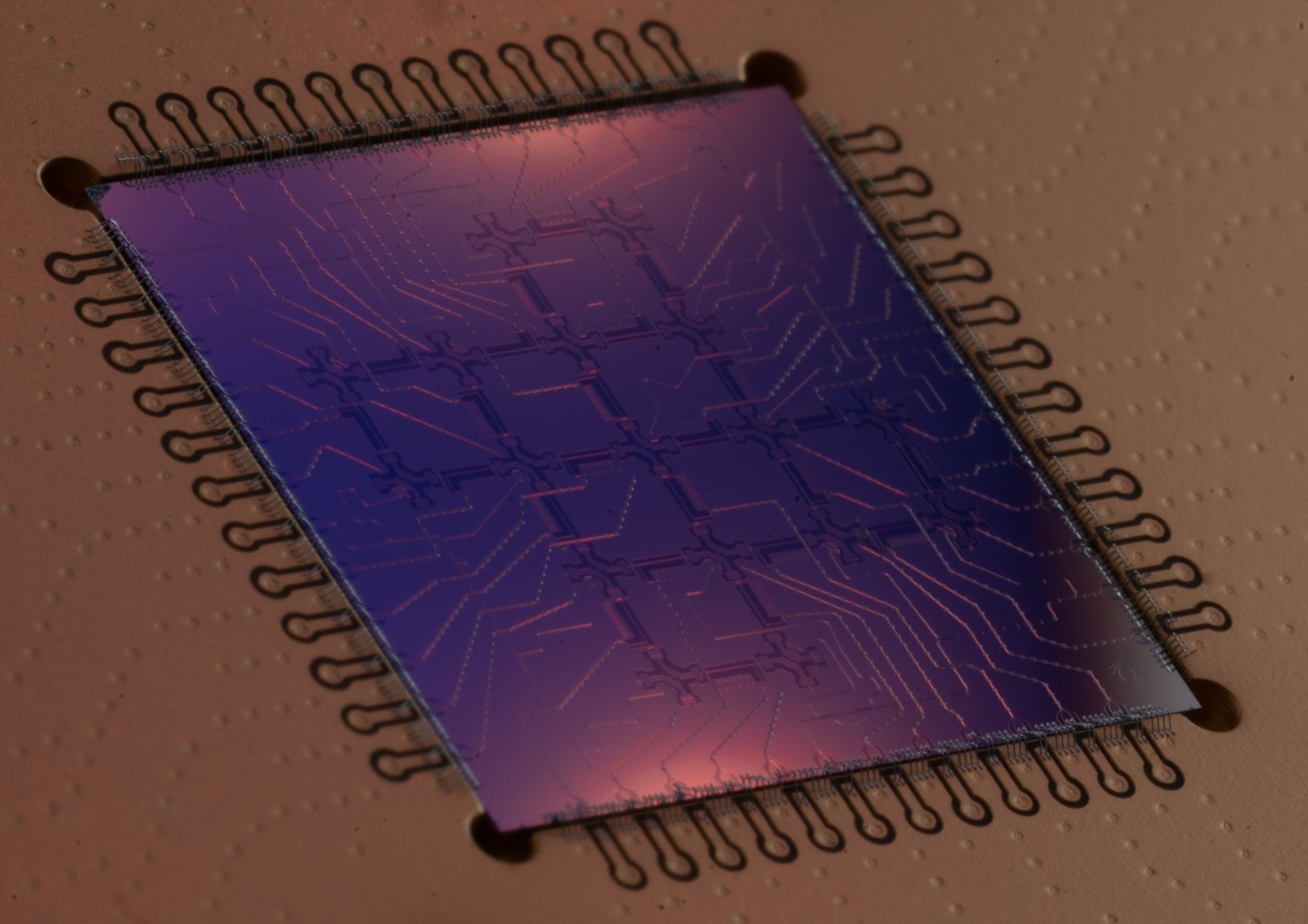
| Project name: | Analyzing novel superconducting materials for superconducting qubits |
| TUM Department: | NAT - Physics |
| TUM Chair / Institute: | E23 - Prof. Stefan Filipp |
| Research area: | Quantum Computing |
| Student background: | Physics |
| Further disciplines: | |
Participation also possible online only: | |
Planned project location: | Walther-Meißner-Institute |
Project Supervisor - Contact Details | |
|---|---|
| Title: | |
| Given name: | Vera |
| Family name: | Bader |
| E-mail: | vera.bader@wmi.badw.de |
| Phone: | +49 (0)89 289 14202 |
Additional Project Supervisor - Contact Details | |
|---|---|
| Title: | |
| Given name: | Lasse |
| Family name: | Södergren |
| E-mail: | lasse.soedergren@tum.de |
| Phone: |
Additional Project Supervisor - Contact Details | |
|---|---|
| Title: | |
| Given name: | |
| Family name: | |
| E-mail: | |
| Phone: |
Project Description | |
|---|---|
| Project description: | Background: |
| Working hours per week planned: | 40 |
Prerequisites | |
|---|---|
Required study level minimum (at time of TUM PREP project start): | 3 years of bachelor studies completed |
| Subject related: | • Basic understanding of solid-state physics and superconducting qubits |
| Other: |